

Kontakt
Dr. Nicki Frank Hinsche
Telefon: 0345 55 25 566
Telefax: 0345 55 25 446
nicki.hinsche@@physik.uni-h...
Raum 0.47
von-Seckendorff-Platz 1
06120 Halle
Forschungsthemen

The current research focus lies on the realistic description of electronic and thermal material properties of nanostructured systems beyond standard Density Functional Theory (DFT).
In detail, I am working on methods and computational implementations to understand, describe and predict electronic and vibronic transport properties in bulk and low-dimensional systems, i.e. single crystals, thin films or monolayers.
Ultimate goal is the multi-scale description of functional devices, based on phenomena like thermoelectrics, superconductivity, multiferroics, phase-change or topological insulators/metals, from the theoretical atomic scale towards the experimentally realisable material.
An overview of the publications can be found at Google scholar and Orcid .
Selected results of the research topics are presented below. Please click the figures for explanations and details.
2D materials
2D materials refer to crystalline solids consisting of a single (or rarely a few) layer of atoms. A major expectation is that, given their exceptional electronic and optical properties, 2D materials will replace conventional semiconductors to deliver a new generation of electronics. Therefor the solid state community is constantly on the pursuit of discovering new 2D materials.
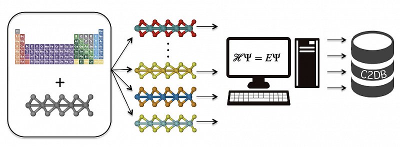
The Computational 2D Materials Database (C2DB) organises a variety of structural, thermodynamic, elastic, electronic, magnetic, and optical properties of around 1500 2D materials distributed over more than 30 different crystal structures. Material properties are systematically calculated by state-of-the-art density functional theory following a semi- automated workflow. The C2DB is fully open and can be browsed online (http://c2db.fysik.dtu.dk ). The C2DB identifies a large number of new potentially synthesisable 2D materials with interesting properties targeting applications within spintronics, (opto-)electronics, and plasmonics. The C2DB offers a comprehensive and easily accessible overview of the rapidly expanding family of 2D materials and forms an ideal platform for computational modeling and design of new 2D materials and van der Waals heterostructures.
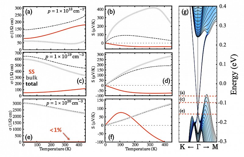
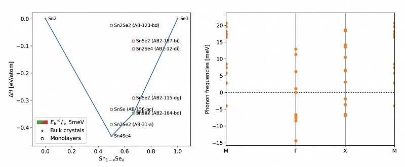
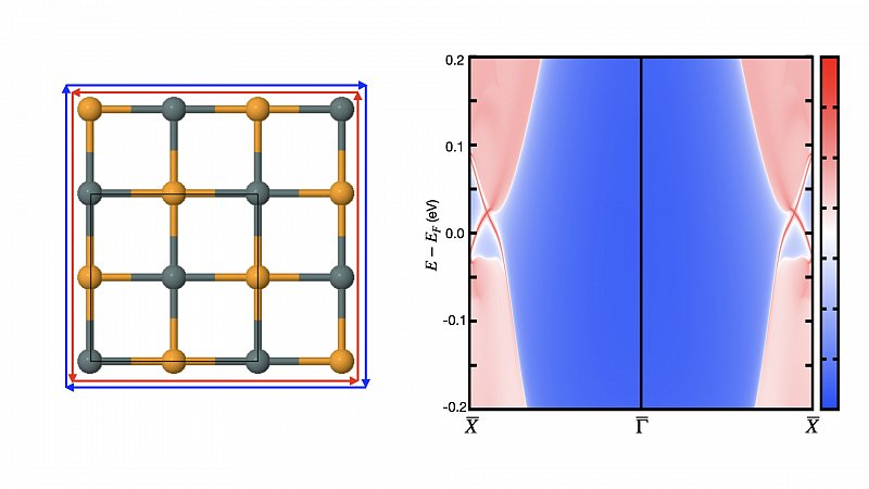
Below an example of cubic 2D SnSe is given. The material was found to be stable on substrates and interestingly possesses topologically protected metallic edge states, while the bulk remains insulating.
Electron-Phonon coupling
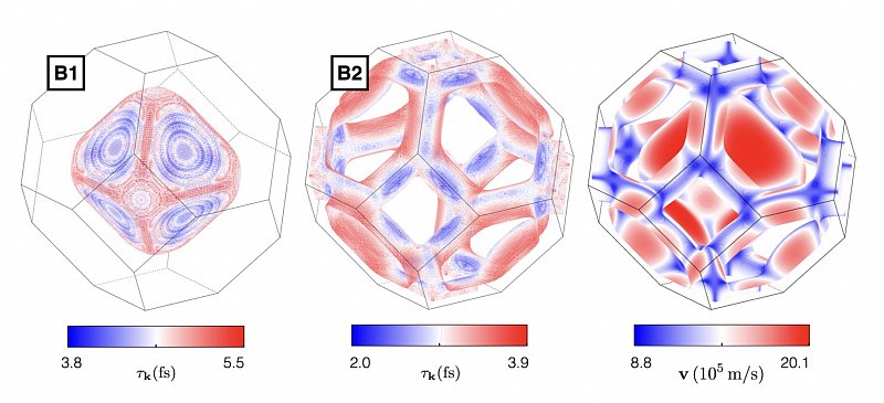
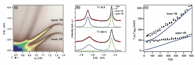
By means of Density Functional Perturbation Theory (DFTP) we are able to calculate the quasiparticle interactions of electrons and phonons (el-ph) as well as phonons and phonons (ph-ph). In particular were focusing on the precise evaluation of the collision integral due to the microscopic el-ph and ph-ph interactions from Fermis golden rule, which then determines the lifetimes of the quasiparticles. The lifetimes and derived quantities are essential to describe phonon-limited transport properties, e.g. the electronic conductivity or the lattice thermal conductivity. A further benefit is the capability to analyze the impact of phonons, i.e. simply said temperature, onto the renormalization of the bandstructure within the diffusive limit.
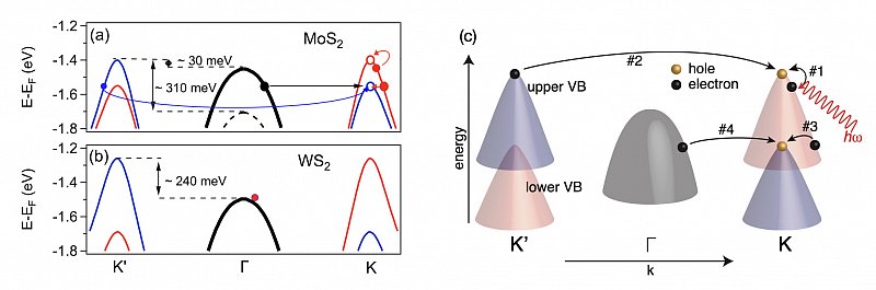
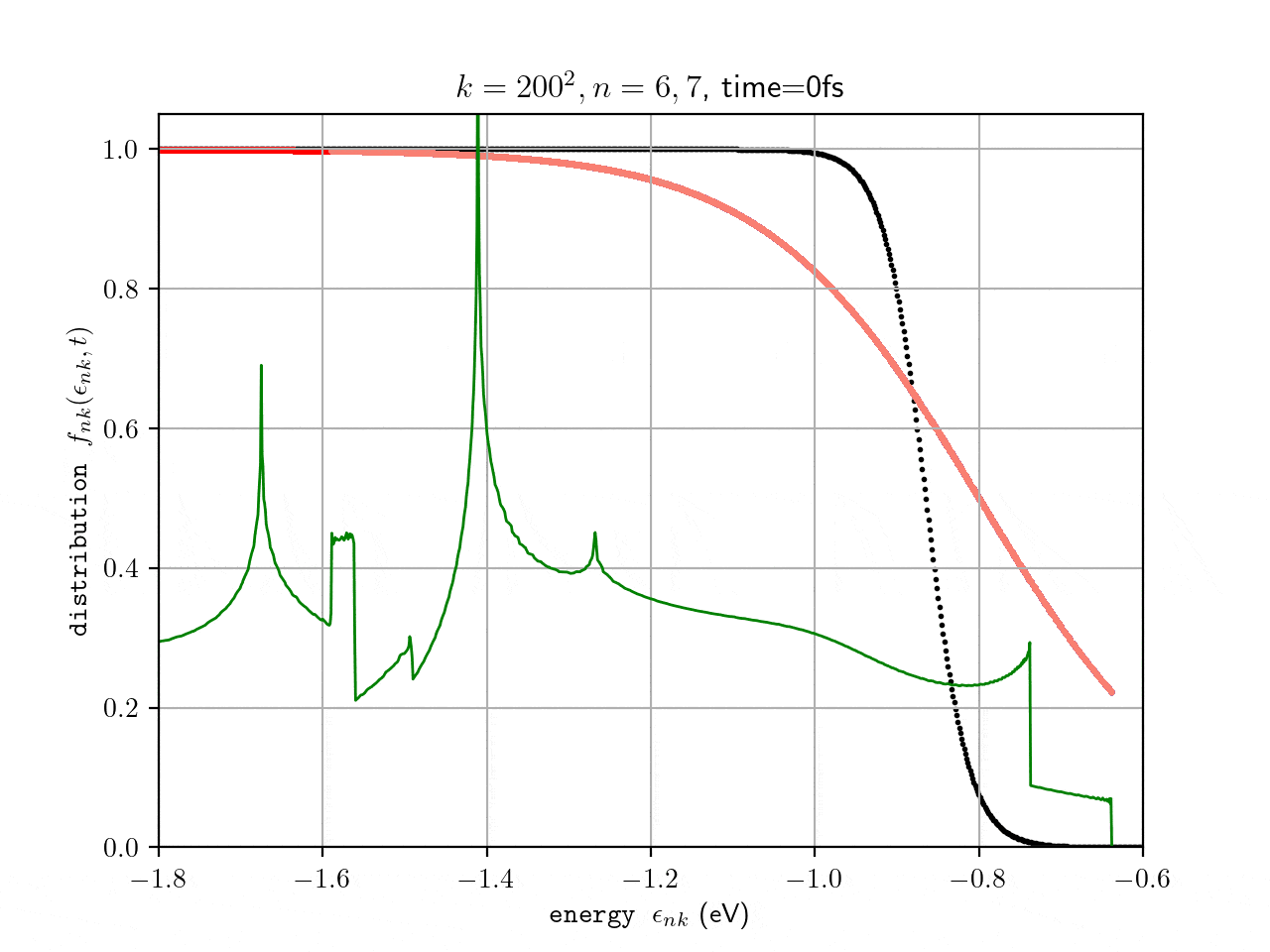
Ultrafast carrier dynamics
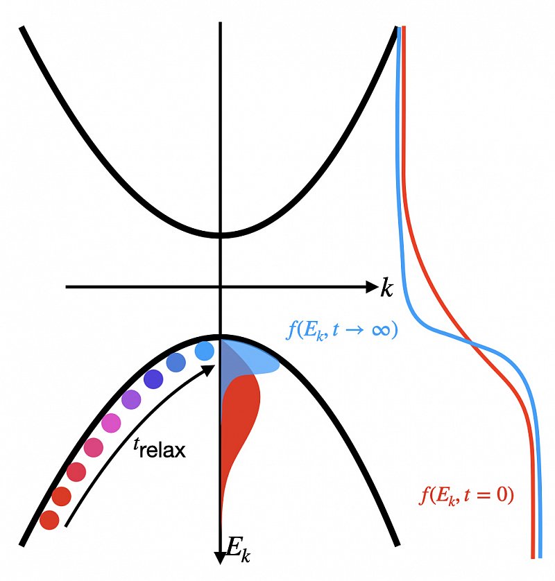
On basis of ab initio derived electron-phonon (el-ph) and phonon-phonon (ph-ph) quasiparticle interactions the time-dependent Boltzmann Transport Equation (tBTE) can be evaluated to describe ultrafast carrier relaxation processes within the first 100s-1000s fs after excitation. Within Blochs Assumption the el-ph and ph-ph tBTE can be decoupled, assuming the phonon system to remain in equilibrium. This approximation already yields very good results on the time-dependent electronic state distribution shortly after thermal or optical excitation. By coupling el-ph and ph-ph tBTE more delicate processes, e.g. the phonon-drag effect, can be calculated at the cost of an elevated computational effort. A theoretical introduction can be e.g. found in Rittweger (2018) .
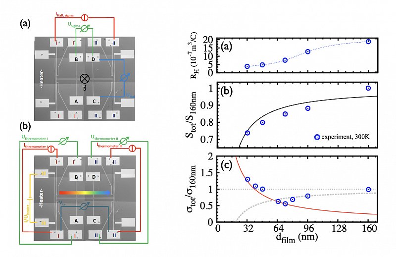
Thermoelectric transport
The research focus lies in understanding the microscopic origin of thermoelectric transport in semiconducting bulk materials, as well as their heterostructures including surface and interface effects.We identify and elucidate mechanisms which could lead to enhanced thermoelectric conversion efficiency. Based on first-principles calculations the electronic structure is determined and lays the foundation to extract the thermoelectric transport properties based on the solution of linearised Boltzmann equations.
Our conceptional ideas were awarded with the Hugo Junkers Prize 2015 for Most innovative proposal in fundamental research (https://www.hugo-junkers-preis.de ), where we conceptionally showed the bottom-up design of a nanostructured, thermoelectric energy harvester, from theoretical DFT calculations towards the working device.
Introductions into our methods from a classical macroscopic thermodynamical or a more advanced quantum-mechanical microscopical ansatz can be found in
- N.F. Hinsche, PhD Thesis "Thermoelectric transport in semiconducting heterostructures", (2013)
- N. F. Hinsche et al. PSSA 213 3 672, special issue on Nanostructured Thermoelectrics, (2016)
- C. Goupil, N. F. Hinsche et al., Thermodynamics and Thermoelectricity, Wiley, 1-74, (2016) - free Chapter 1