

Fields of Research
The group focuses on solar cells that are based on chalcogenide thin films. Light absorbing layers of the type Cu(In,Ga)(Se,S)2, Cu2ZnSn(Se,S)4 or other chalcogenides are combined in a thin film heterostructure similar as shown in Fig. 1. Research topics are:
- Improving the efficiency of state-of-the-art solar cells, mainly Cu(In,Ga)(Se,S)2
- Understanding current efficiency limitations
- Investigating process schemes for high productivity and low cost
- Testing in-line and off-line process monitoring and quality assessment
- Develop new heterostructure components, in particular absorber layers
- Modelling of electronic transport
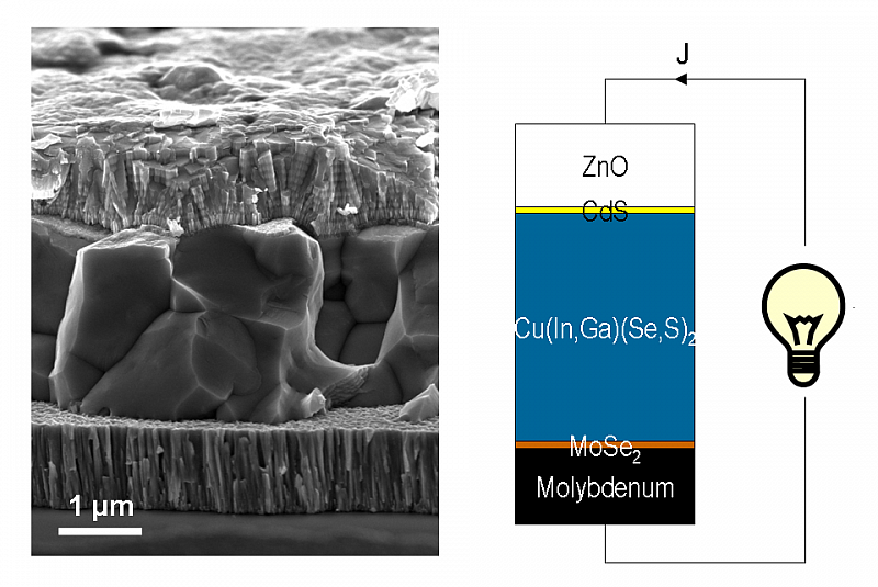
Fig. 1 Scanning electron micrograph of a Mo/Cu(In,Ga)Se2/CdS/ZnO solar cell on glass in cross-section view. Thin layers of MoSe2 (~10 nm) and CdS (~50 nm) are not visible in the micrograph. The working principle of heterostructure solar cells is simple: Due to the asymmetric contacts (CdS/ZnO on one side and Mo on the other side) electrons and holes being the charge carriers are flowing to opposite directions. They form the photo current which can drive an electrical load.
Thin film preparation in our group uses physical vapour deposition under vacuum – a technique that is also employed in commercial production. Different elemental vapours are directed to the heated substrate (Fig. 2). Insitu monitoring techniques such as laser light scattering give a real-time signal of the growing thin-film. Different substrate types can be used. In the system of Fig. 2 only the absorber layers such as Cu(In,Ga)Se2 are prepared. Other deposition methods for the cell in Fig. 1 are sputtering (Mo, ZnO) and chemical bath deposition (CdS) which are performed in different set-ups. The thin MoSe2 layer is a reaction product of the polycrystalline molybdenum film with the selenium atmosphere.

Fig. 2 Sketch of a physical vapour deposition system for the simultaneous evaporation of different elements. Typically non-crystalline substrates are used which lead to polycrystalline film growth. Epitaxial growth requires crystalline substrates and is only occasionally accomplished for research purposes.
Another aspect of research is quaternary semiconductors based on copper, zinc, tin and sulphur or selenium (so-called kesterites). They can be an interesting alternative to conventional absorbers for thin-film solar cells, as their starting materials are non-toxic and available in large quantities on earth. In the specialist group, absorbers made of kesterites are developed and the properties of solar cells made from them are investigated (Fig. 3). A PVD system is also available for this purpose, in which the thin layers are deposited by means of thermal co-evaporation. This is combined with an X-ray diffractometer, which enables an in-situ investigation of the layer formation processes.
The focus is in particular on:
- the investigation of the processes of layer formation by means of in-situ and ex-situ methods
- the development of new preparation paths with improved layer properties
- the development of procedures for in-situ process control
- the investigation of the loss mechanisms of kesterite solar cells
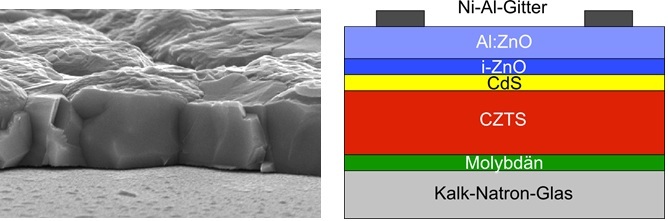
Fig. 3 shows the cross-sectional scanning electron micrograph of a Cu2ZnSnSe4 (CZTS) absorber layer on the left and the structure of a CZTS solar cell on the right.
The main research areas are worked on in various projects, including:
- "Alkali-induced surface defects and interface passivation in chalcogenide solar cells" (DFG 2019 - 2026)
- “Stable Inorganic TAndem solar cell with superior device efficiency and increased durability- SITA” (European Union 2022 – 2025)
- "Perovskite thin-film solar cells from multi-stage dry reaction processes" (DFG 2022 - 2025)
- „High efficiency bifacial thin film chalcogenide solar cells”, Acronym: Hi-BITS (European Union 2023 – 2026)